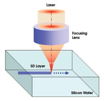
Laser Dicing Silicon Wafer
Laser Dicing Technique Cuts Wafers From The Inside Out Features Jan 2008 Photonics Spectra

Stealth Laser Dicing Youtube
.jpg)
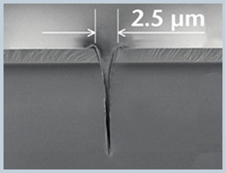
Wafer Analysis Of Laser Grooving
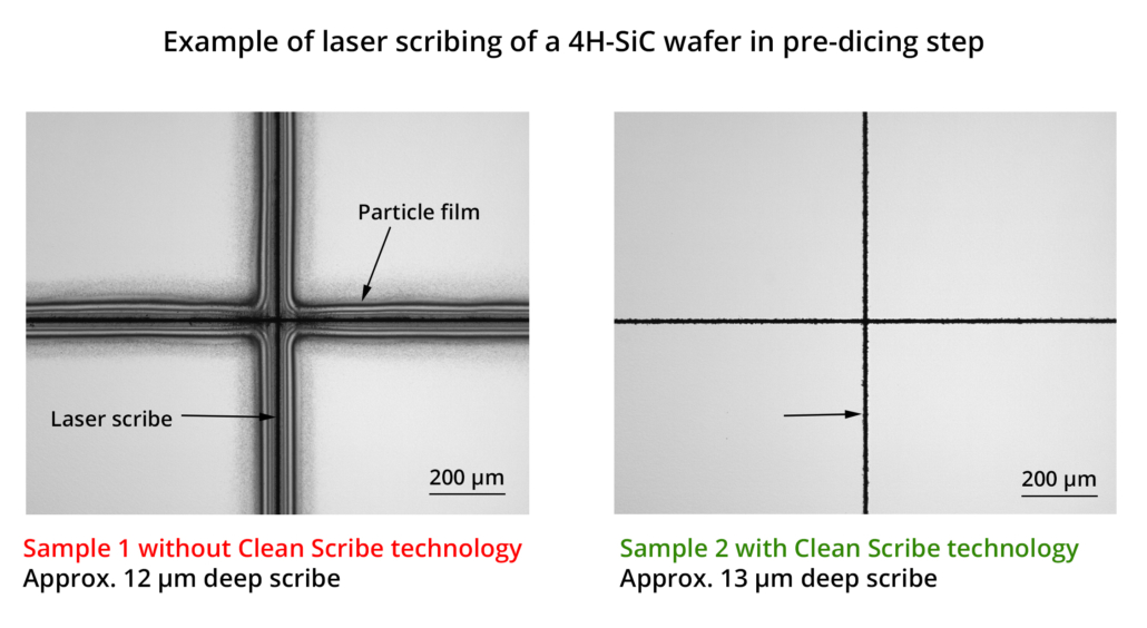
3d Micromac Unveils Clean Scribe Technology On Microdice Tls Laser Dicing System For Low Cost Particle Free Dicing Of Silicon Carbide Wafers Laser Micromachining 3d Micromac Ag

At Dsk Technologies Silicon Dummy Mechanical Grade Wafers Are Available In Sizes From 2 To 12 Diameter This Silicon Dummy Wafer Is Dummy Wafer Web Design

Silicon Wafer Dicing All Diameters 27 Years Of Experience Svm

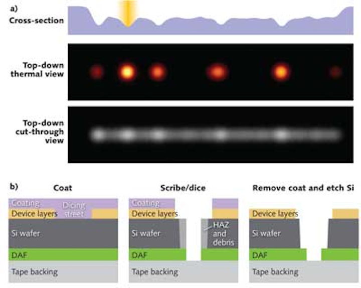
Demonstration of cutting features into 1 5 mm thick silicon wafers using a laser micromachining system equipped with a qcw laser.
Laser dicing silicon wafer.

Multilayer Stack Materials On Silicon Based Wafer Dicing Processes Using Ultraviolet Laser Direct Dicing And Milling Methods Sciencedirect
Microelectronics Processing Zero Overlap Laser System Speeds Ultrathin Wafer Dicing Laser Focus World

Laser Dicing Wafer Cutting By Laser Microjet Ppt Video Online Download

Wafer Resizing Coring Mems Laser Marking Laser Machine

Laser Process Wafer Wafer Marking Wafer Dicing Wafer Cutting Wafer Scribe Youtube

Chuck Table Chucks Ceramics Black And Brown

Dsk Technologies What Matters Is Choosing The Right Companies Like Dsk Technologies For Picking The Right Electronic Parts The Co In 2020 Tape Wafer Electronic Parts
Laser Dicing Silicon

Laser Processing Of Doped Silicon Wafer By The Stealth Dicing Semantic Scholar

Mold Cleaning Rubber Sheet Looking For An Efficient Solution For Mold Sheet Cleaning Read Here For The Dsk Technologies With Images Mold Release Molding Led Manufacturers

Silicon Mems Micromachining And Patterning Mems Laser Machine Detector
Semiconductor Production Support With Fiber Lasers Spi Lasers

Trial To Cut Silicon Wafer With Laser Cutter Youtube

Laser Dicing Silicon

For System Integration And Shop Service Laser Resistor Trimming Of Thick And Thin Film Hybrid Microelectronic Devices Active An Resistors Thin Film Graphing

Microdice Wafer Dicing System For Sic Youtube

Silicon Wafers Producers And Suppliers Company Semiconductor Materials Wafer Semiconductor
Laser Scribing Sapphire Silicon Carbide Wafer Scribing
1
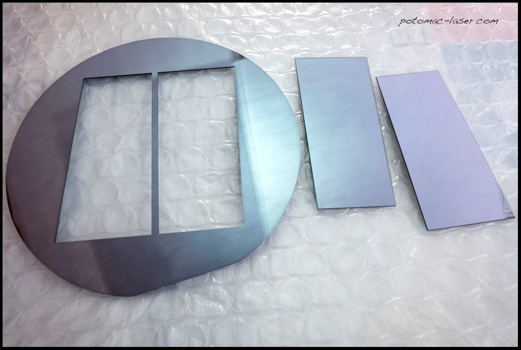
Rapid Dicing Of Silicon Wafers Potomac Photonics Fablab Examples

Figure 3 From Uv Laser Dicing Without Failure Caused By Contamination And Heat For Thick Anodically Bonded Silicon Glass Mems Wafers Semantic Scholar

The Mechanism Of Wafer Dicing Process The Water Jet Guides The Laser Download Scientific Diagram

Figure 1 From Uv Laser Dicing Without Failure Caused By Contamination And Heat For Thick Anodically Bonded Silicon Glass Mems Wafers Semantic Scholar

Laser Dicing Solutions Disco Laser Features Advantages Disco Corporation
Source : pinterest.com
