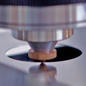
Laser Cutter For Silicon Wafer
Silicon Wafer Cutting Microholes Laser Drill Silicon Cutter

Micromachining A Silicon Wafer Laser Impressions Inc

Trial To Cut Silicon Wafer With Laser Cutter Youtube
Laser Dicing Technique Cuts Wafers From The Inside Out Features Jan 2008 Photonics Spectra

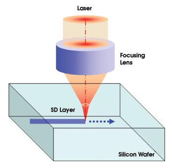
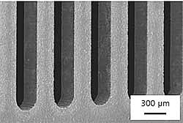
27 Laser Cut In Silicon Wafer Using 1064 Nm Wavelength Download Scientific Diagram

Silicon Wafers Laser Micromachining Silicon Wafer Cutting
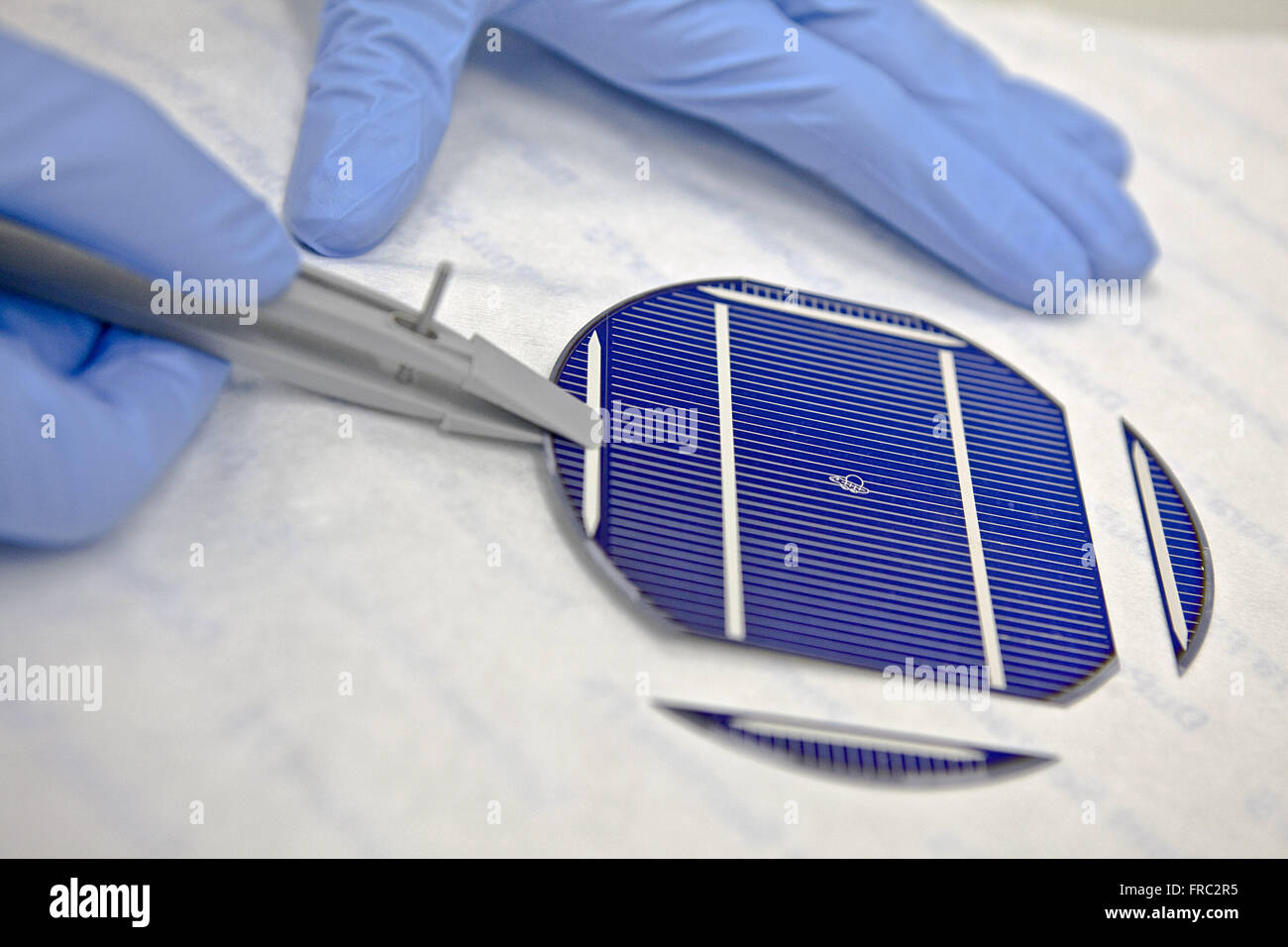
This is usually followed by a mechanical breaking procedure to produce silicon rectangular tiles for subsequent operations he mechanical break will follow allowing the scribing line offering the least path of resistance.
Laser cutter for silicon wafer.

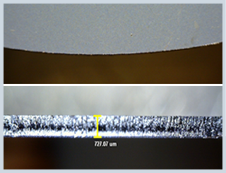
Cross Sections Of Silicon Wafers Cut By Different Techniques A By Download Scientific Diagram

Laser Cutting Silicon Wafers
Micro Laser Cutting Sapphire Diamond Ceramics Metals

Si Silicon Laser Processing Cutting Drilling
Scientist Manipulating Silicon Wafer During Laser Cutting Of The Same Stock Photo Alamy
Silicon Wafer Cutting
Laser Cutting Silicon Solar Cells

Wafer Resizing Coring Silicon Mems Laserod
Fiber Laser Cell Solar Silicon Wafers Scribing Cutting Dicing Easy Operation

Pre Crack Laser Thermal Cracking Method For Cutting Asymmetric Cutting Download Scientific Diagram

Fiber Laser Cutting Of Silicon Spi Lasers

China Silicon Wafer Cutting Machine Wafer Dicing Laser Scriber China Laser Cutter Fiber Cutter

Laser Dicing Wafer Cutting By Laser Microjet Ppt Video Online Download

Jg16b China Pico Laser Cutting System For Silicon Wafer Scribing Manufacturer Supplier
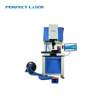
Perfect Laser High Quality Silicon Wafer Solar Cell Laser Cutting Dicing Scribing Machine Buy Laser Dicing Silicon Wafer Silicon Wafer Laser Scribing Machine Solar Cell Laser Scribing Machine Product On Alibaba Com

Multilayer Stack Materials On Silicon Based Wafer Dicing Processes Using Ultraviolet Laser Direct Dicing And Milling Methods Sciencedirect
Fine Laser Cutting Of Silicon Wafers Design For Laser Manufacture
Solar Cell Laser Cutting Machine Germany Ipg Silicon Wafer Solar Cells Scribing Cutting Machine Buy Ipg Solar Cell Laser Cutting Machine Silicon Wafer Laser Cutting Machine Solar Cell Cutting Scribing Machine Cutter Product On Alibaba Com
Leather Laser Cutting Machine Price Product Printer Laser Ltt Buy Leather Laser Cutting Machine Price Laser Product Laser Cut Printer Ltt Laser Product On Alibaba Com
Best Laser Cutting Drilling Experts Laserod By Laserod Wafer Medium

Wafer Alignment And Dicing Process A Silicon Wafer With Sputtered Download Scientific Diagram
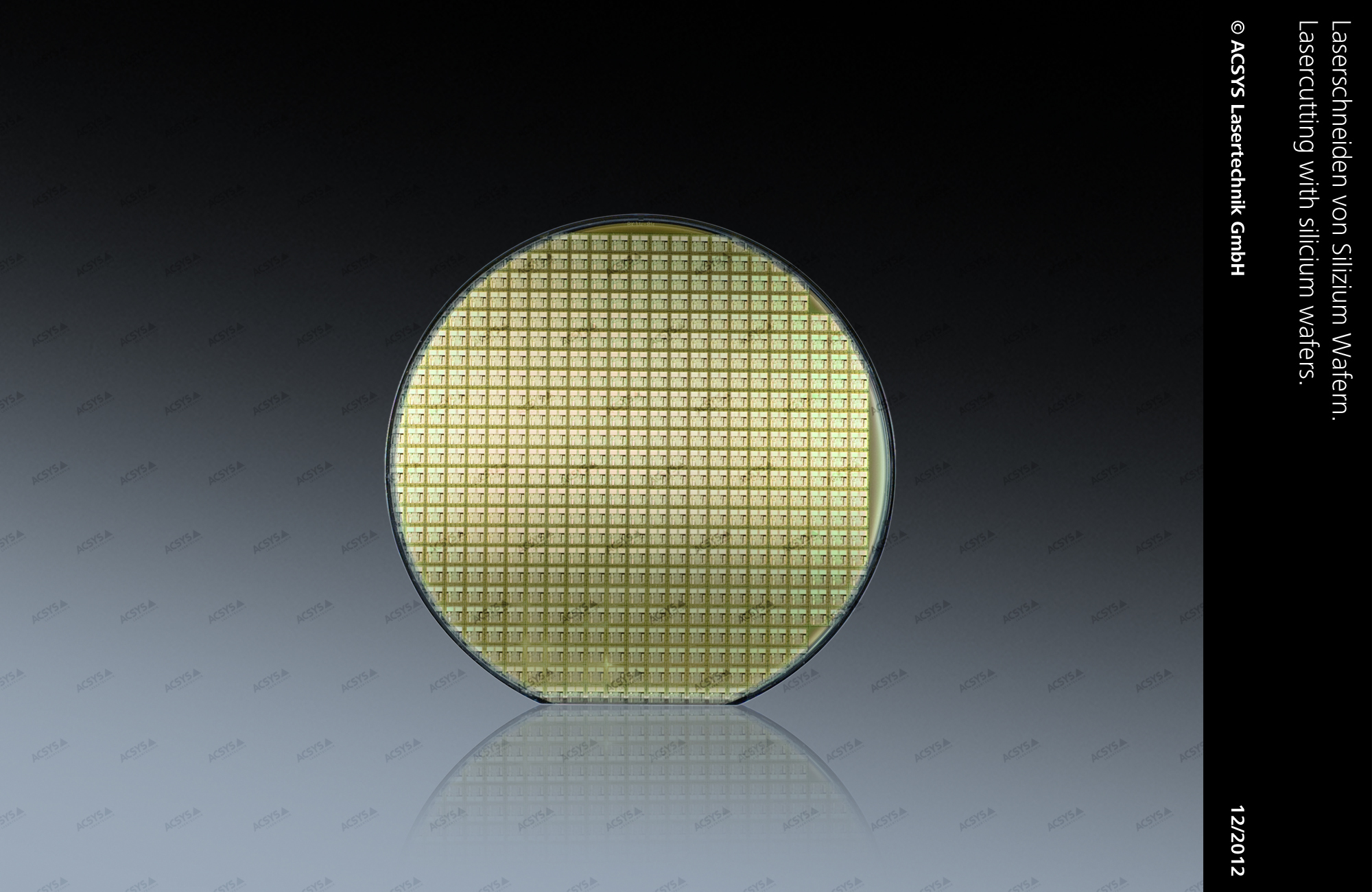
Applications Laser Cutting Acsys Lasermaschinen

China Keyland Pv Cell Manufacturing Solar Module Making Equipments Silicon Wafer Solar Cell Laser Cutting Machine China Solar Cell Laser Scribing Machine Solar Cell Cutting Machine

China Silicon Wafer Cutting Machine Solar Machine Cutting Solar Cells China Laser Cutter Fiber Cutter
Source : pinterest.com
